
The technology of High Density Interconnect (HDI) is rapidly gaining prevalence and importance in the designing of printed circuit boards. A growing number of fields are integrating HDI technology into their respective products.
What is High-Density Interconnect (HDI) Technology?
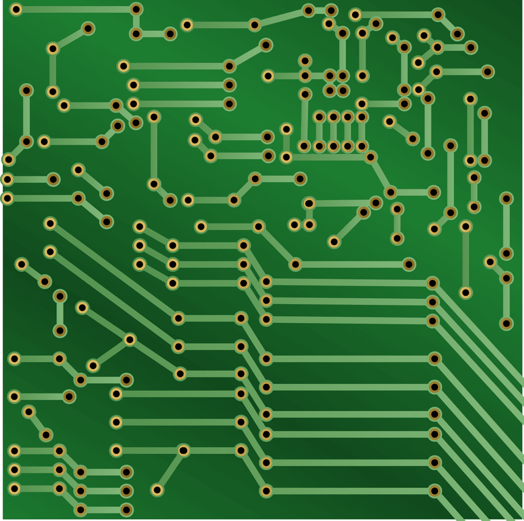
With the aid and assistance of HDI technology in PCB designing, the construction becomes quite dense on a board as much smaller components are put together in close distance to each other resulting in shorter paths between various parts. Shorter paths mean signals are transmitted quite fast and factors such as signal loss and crossing delays are drastically reduced.
What are the Benefits of High Density Interconnect (HDI) Printed Circuit Boards?
Numerous benefits are associated with HDI PCBs which are outlined below:
- Consolidated Design:
Talking about vias; High Density Interconnect printed circuit boards normally use blind vias, buried vias or a combination of both. Even micro vias, which possess a drastically small diameter, are also utilized in High Density Interconnect PCBs. This gives the PCB designer a lot of space in his/her hands to place the components. Moreover, the usage of above-mentioned vias in designing a HDI PCB; also enables a PCB designer to place more components on a single printed circuit board as the designer is having enough space available with him.
- More Dependability:
Certain conditions are pretty extreme for an equipment to operate. High Density Interconnect printed circuit boards, when multi-layered, provide a strong stacked vias interconnection. This strength is sufficient for equipment, in which HDI PCBs are used, to operate in extreme conditions and give the required and expected the level of performance.
- Much Better Transmission of Signals:
Much smaller components are used in a High Density Interconnect printed circuit board. Moreover, since the components are placed much closer to each other as compared to the traditional PCBs, signal losses and the chance of cross delays is drastically reduced. Hence, the HDI PCB performs much better, in terms of signal transmission, as compared to the traditional PCBs, thereby making them a preferable choice in a variety of applications.
- Cost-Effective & Affordable Design
As we can see, in the case of High Density Interconnect PCBs; the overall size of the final board is reduced. This size-reduction doesn’t result in any kind of loss in terms of quality. Hence, a good quality printed circuit board can be designed at a price which is well within the estimated budget of the client. Working within the boundaries of the budget set by the client and delivering an ultimate quality product will undoubtedly make your client extremely happy with your work compelling him to look for your services as and when he requires the same, giving your business a much-needed boost in terms of quality and client satisfaction.
- Extraordinary Versatility
High Density Interconnect printed circuit boards are employed and utilized in a variety of different applications in which there are non-negotiable concerns regarding weight, space, quality, performance, and dependability.
Are there any Limitations of the High Density Interconnect (HDI) Technology?
There are certain limitations to the HDI technology. The major one being the cost of the equipment required to manufacture HDI printed circuit boards.
Special methods, the most important one being Laser Direct Imaging + forbes (LDI), are used in the manufacturing of HDI boards. LDI is used in the fabrication process of the HDI PCB due to the presence of fine lines on the board. Along with fine lines, the tighter spacing of the components, make Laser Direct Imaging, an absolute essential, in the fabrication process of the High Density Interconnect PCBs. There is a significant amount of expense in acquiring the LDI equipment and machinery.
Along with the cost of the equipment; the person, who is responsible, for handling and operating the equipment, needs to be trained thoroughly before handing him over the complete responsibility of the equipment.
Post going through the above-mentioned limitations; it can be safely said that the number of advantages, undoubtedly, overcome and eliminate the presence of these drawbacks.
Conclusion
High Density Interconnect PCBs, owing to their numerous benefits, are being used in a number of different fields, the major ones being medical equipment, aerospace, computers, and smartphones as well as in several devices used in military communication. Apart from these, there are myriad of other areas where HDI PCBs are used, making them immensely popular.


